
ZENIT SMART POLYCRYSTALS
Polycrystals for innovative applications

About us
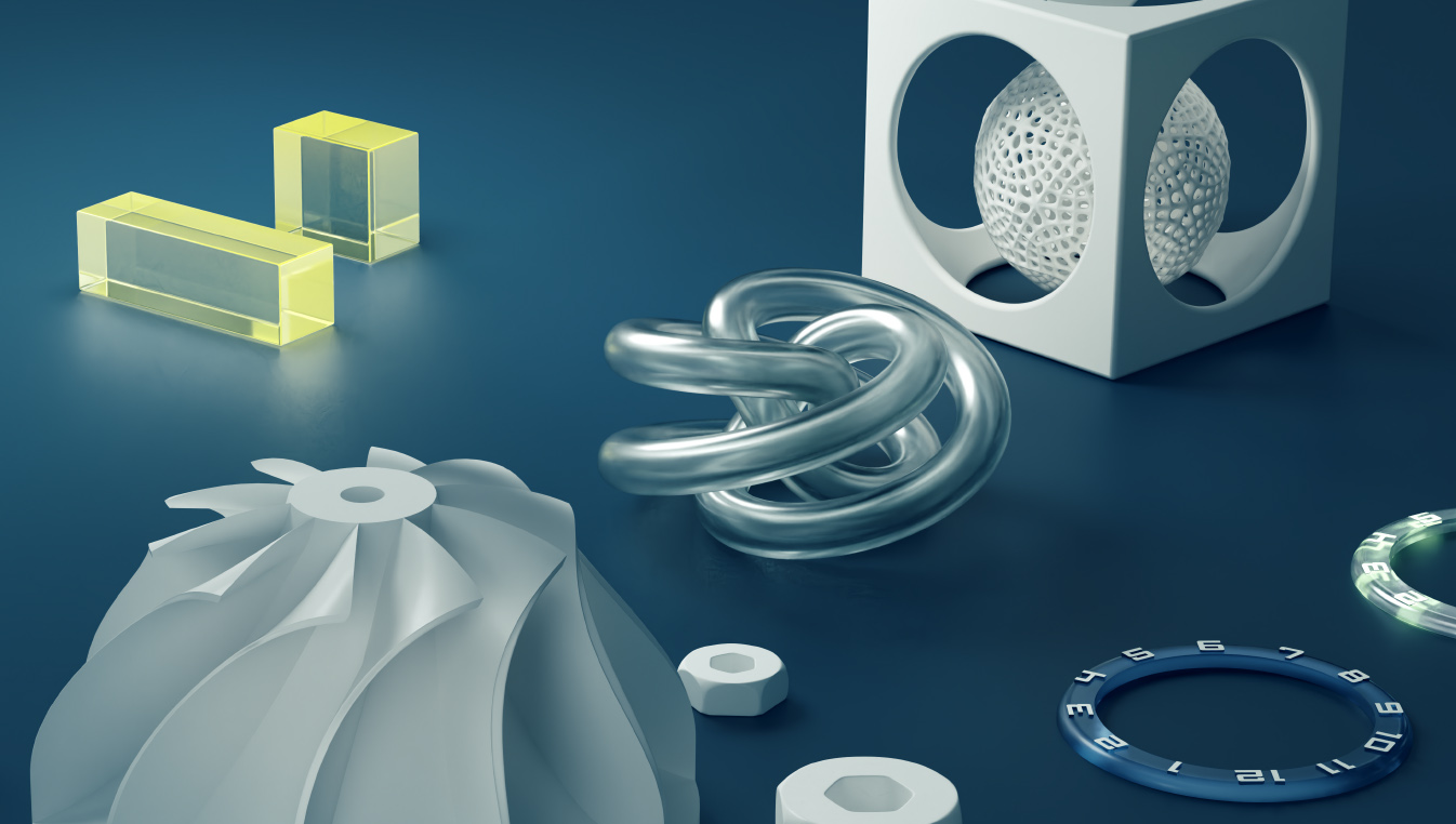
Zenit Smart Polycrystals manufactures polycrystalline ceramic components tailored to specific customer requirements. Zenit’s manufacturing process uses a patented technology based on ceramic 3D printing, enabling a high degree of freedom in both shapes and compositions. Various markets — including laser systems and semiconductors — can benefit from Zenit components.
EXECUTION STRATEGY
• Feasibility studies
• Participation in international and EU projects
• Manufacturing of standard and tailored products
• Collaborative development of components to enhance performance
Competitive advantage

ENHANCED HEAT DISSIPATION EFFICIENCY

FLEXIBLE SHAPE AND COMPOSITION IN ALL THREE DIMENSIONS

REDUCED PRODUCTION COSTS

ENHANCED PERFORMANCE ACROSS A WIDE RANGE OF APPLICATIONS
Zenit Smart Polycrystals manufactures highly dense and transparent polycrystalline ceramic components tailored to specific customer requirements. Zenit’s manufacturing process uses a patented technology based on ceramic 3D printing, enabling a high degree of freedom in both shapes and compositions, including gradients.
Zenit Smart Polycrystals manufactures highly dense and transparent polycrystalline ceramic components tailored to specific customer requirements. Zenit’s manufacturing process uses a patented technology based on ceramic 3D printing, enabling a high degree of freedom in both shapes and compositions, including gradients.
ENHANCED HEAT DISSIPATION EFFICIENCY
FLEXIBLE SHAPE AND COMPOSITION IN ALL THREE DIMENSIONS
REDUCED PRODUCTION COSTS
ENHANCED PERFORMANCE ACROSS A WIDE RANGE OF APPLICATIONS

The Zenit Smart Polycrystals laboratory
The Zenit Smart Polycrystals laboratory
The target market is vast and continually growing

Laser
To the solid-state laser systems market, Zenit offers laser gain media formed by polycrystals in alternative to traditional single crystals. Zenit polycrystals help dissipate more effectively the heat generated during the emission process, thus minimizing degradation of performance caused by thermal gradients and their related optical effects. This is made possible by the type and distribution of dopant ions within the component volume, which can vary in three dimensions.

Semiconductors
For the semiconductor industry—specifically in plasma etching of silicon wafers—Zenit supplies yttrium aluminium garnet (YAG)-based nozzles and injectors. These components offer superior corrosion and chemical resistance compared to traditional alumina-based alternatives and can be custom-designed to meet specific application requirements.
Advanced applications
Zenit produces polycrystalline components for a wide variety of applications, including scintillators and industrial processing and applications, combining high mechanical and thermal resistance, chemical inertness , with complex shapes and multiple compositions.
News
ZENIT SMART POLYCRYSTALS